Application
3D Package
3D Package
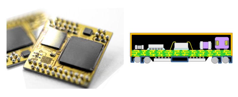
At present, the investment cost of 5nm/3nm advanced process of semiconductor chips is high, and it is getting closer and closer to the limit. The improvement of chip performance through advanced 3D packaging has attracted more and more attention from the industry. With the maturity of various packaging technologies such as System in Package (SiP), Chip to Wafer (CoW), and Wafer level Package (WLP), 3D packaging has become an increasingly trend.
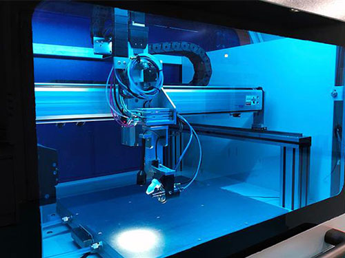
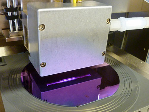
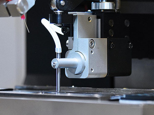
Changzhou Wellsin-Semi Equipment Co., Ltd. provides solutions for 2.5D/3D packaging from the perspective of equipment, mainly including flux/EMI spraying, atmospheric plasma surface treatment, bumping flip chip bonding and other technologies. Our solution can effectively improve packaging. Quality and cost reduction, welcome to inquire!
Related Products
-
 Mobile Site


